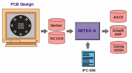


Using IPC-D356 to Import Nets and Nodes


Since Gerber data has no net or node information, the output from NETEX-G will
not include the net names and node (or pin) names assigned by the board
designer. However if the simulation engineer is provided with an IPC-D-356 file
by the board designer, then this file can be imported by NETEX-G and net names
and pin names can be extracted from it.


What is IPC-D-356?


IPC356 is a file format specification created by the IPC that defines test
points on a board and is used to create test programs and test fixtures for the
PCB. It is in ASCII column format and includes net names, pin and reference
designators, coordinates and type of test point. Most PCB design software can
export this file as it is very useful and requested by the PCB manufacturer.
The original IPC356 has been updated so that there is both IPC356A and B
versions in use. NETEX-G can read either version. A sample is shown below:


P JOB BPN 710064-0001
P UNITS CUST 0
P VER IPC-D-356A
P IMAGE PRIMARY
317+3.3V J13 -2 D0400PA00X+043550Y+006480
327+3.3V C171 -1 A01X+041900Y+006660
327+3.3V D1 -3 A08X+040650Y+007720
317BSP_R0_B5 VIA D0098PA00X+023895Y+022535
327BSP_R0_B6 R335 -1 A08X+024140Y+022050
327BSP_R0_B6 U26 -35 A01X+030400Y+019515
327BSP_R0_B6 R334 -1 A08X+023733Y+022050
327GND C215 -2 A08X+050850Y+047799
327GND C415 -2 A08X+025278Y+008183
327PCI_CLK J1A1 -25 A01X+028198Y+000600
327PCI_CLK U26 -46 A01X+030715Y+015735
999


Generally speaking, the test points defined by IPC-D-356 are either on the top
or bottom of the PCB. In this example, A01 is the first layer and A08 is the
bottom layer. The first 3 characters define the type of test point, followed by
the net name. You can see the reference designator information followed by a
pin number for components. You can also see a via which has no ref designator
or pin but for which the pad size is described.


