
|
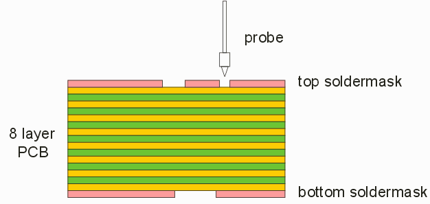
SilhouetteSilhouette is a special function added to NETEX-G whose primary users are those who are creating 3D models for purposes of probe card design and modeling. It is normally used to remove all geometry from inner PCB layers. Imagine that you have a multi-layer PCB (say 8 conductor layers) with layout data in ODB++. You want to build your probe card using a 3D modeling software such as SolidWorks. So you want an accurate 3D model of the top side of the board and the bottom side of the board. You will want the solder masks as part of your 3D model since you don't want to accidentally drop a probe tip onto the solder mask. 
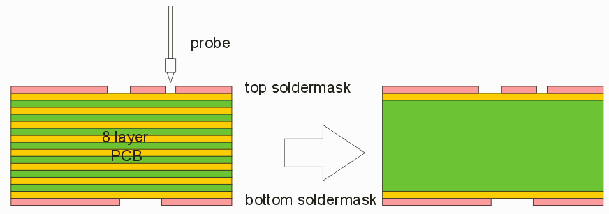
What you don't want or need is all the inner layer geometries. All the complex geometry on those inner layers will make your 3D file so large that your modeling software will choke on the data. One way to eliminate the unwanted detail is to simply delete all the inner layers in your stackup and replace them (and their associated dielectrics) with a single "fat" dielectric as shown below. Then when you run NETEX-G with a 3D output, you will only get geometry from the top and bottom etch layers.  The problem with this approach is that the user has to manually re-compute the correct value of the "fat" dielectric or the board thickness will change significantly. The silhouette directive eliminates the need for this.When it is used, any conductor layer that is "redefined" as a silhouette will not have all its geometry processed and sent to the output of NETEX-G. Instead, NETEX-G will use the PROFILE information to define the boundary of a single body representing the conductor on that layer. This keeps the resulting 3D output file (3Di format) as small as needed to describe just the layers that were not silhouetted. |
Download |
Benchmark Files |
Revision History |
Price |