References for DMD based Direct Lithography
Below are some references -- papers and patents -- that are of interest to using DMD for direct exposure of PCBs and other microelectronic substrates.
WEB Sites
TI - DLP & MEMS Digital Light Exposure
Papers and Application Notes
Eric J. Hansotte, Edward C. Carignan, W. Dan Meisburger, High speed maskless lithography of printed circuit boards using digital micromirrors, Maskless Lithography, Inc., 2550 Zanker Road, San Jose, CA 95131
Ljungblad, U., Sandstrom, T., Buhre, H., Durr, P.,Lakner, H., New Architecture for laser pattern generators for 130nm and beyond, Proc. SPIE 4186 (2001).
Michigami, N.,Yamaga, M., Kawamura, M., Kuze, O., Nakamura S., High-performance Printed Circuit Board Production Equipment for Ultra High Density Multi-layer Wiring., Hitachi Review, Vol. 60 (2011) No.5 pp 216-221
Hoonchul Ryoo, Dong Won Kang, Yo-Tak Song, Jae W. Hahn, Experimental Analysis of Pattern Line Width in Digital Mask Lithography, Journal of Micro/Nanolith MEMS MOEMS 11(2) 023004 (JUN 01,2012)
Kwang-Ryul Kim, Junsin Yi, Sung-Hak Cho, Nam-Hyun Kang, Myung-Woo Cho,Bo-Sung Shin, Byoungdeog Choi SLM-based maskless lithography for TFT-LCD, Applied Surface Science, Volume 255, Issue 18, 30 June 2009, Pages 7835–7840
D.-H. Lee, Optical system with 4 ìm resolution for maskless lithography using digital micromirror device, J. Opt. Soc. Korea 14, 266-276 (2010).
Maskless Exposure Technique see summary below ...
Patents
There are, of course, a large number of patents for direct imaging using DMD/DLP micromirror technology and they seem to go back to about 2001. Here are some that appear to be of interest. Our interest at Artwork is in data prep and the amount of data (bits), how they have to be arranged for DMD applications and how fast they have to be delivered.
US Patent 7969636 June 28, 2011, Hitachi Via Mechanics PDF
Laser direct imaging apparatus - does not use a DMD but instead a rotating polygonal mirror.
US Patent 7167296 January 23, 2007 Maskless Lithography, Inc. PDF
References a spatial light modulator and a continuous moving photosensitive substrate.
US Patent 7295362 November 13, 2007 Maskless Lithography, Inc. PDF
References a spatial light modulator and a continuous moving photosensitive substrate. Simiar to previous but refers to blurring to to enable sub pixel resolution; claim 48 includes:"wherein the direction of movement of said image is not parallel to columns of pixels in said projected image of said spatial light modulator."
US Patent 7508570 March 25, 2009 Maskless Lithography, Inc. PDF
References a spatial light modulator and a continuous moving photosensitive substrate. Simiar to previous but refers to blurring to to enable sub pixel resolution;
US Patent 7639416 December 29, 2009 Maskless Lithography Inc. PDF
See above ...
US Patent 6379867 Jan 10, 2000 Ball Semiconductor PDF
Older approach to creating images using a pixel array. Not continuous motion of the substrate ...
US Patent 6425669 Jul 30, 2002 Ball Semiconductor, Inc. PDF
Early patent using an array such as digital mirror or LCD to create pattern.
US Patent 673237 B2 Oct 29, 2002 Ball Semiconductor, Inc. PDF
A solid patent on the direct lithography with pixel panel (i.e. DMD) and scanned substrate.
US Patent 6870604 B2 March 22, 2005 Ball Semiconductor, Inc. PDF
Describes very clearly the point array method and computations for rotating the DMD.
The "Point of Array" method
Japan Science Engineering Co. Ltd (DNK)
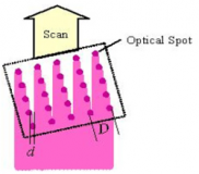
A microlens array is employed so that each microlens condenses a square beam from the DMD's corresponding pixel into a smaller round spot.
The beam spots are arranged in rows making a certain angle with their scanning direction above the imaging plane. The spots that scan in slightly different positions achieve the imaging resolution higher than the DMD's pixel size wihtout sacrificing the size of the exposing field.
For example, when the optical magnification ratio is 5:1, an imaging resolution of 0.05um is possible.

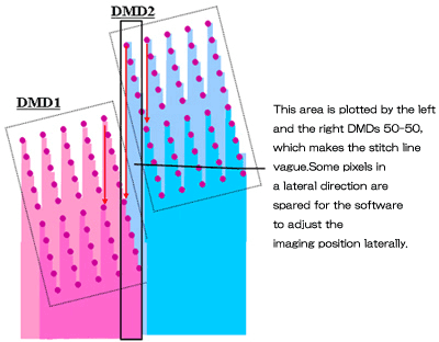
Invisible stitch between scan images
In the "Point of Array" method, the stitching area between two scan images are plotted 50-50 in the respective left and right scan images. In combination with an imaging-position adjusting capability, it makes the stitch less distinctive.

