Next - Notes on matching the existing pattern on the wafer and openings ....

Wafer and Die Setttings
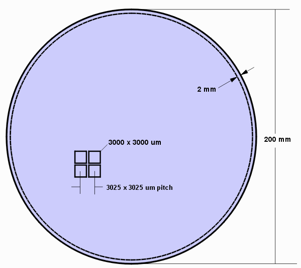
In this example we are working with: a) a 200 mm diameter wafer b) an exclusion zone of 2.5 mm at all edges of the wafer c) a die of 3000 x 3000 um with a street width of 50 um You can see a simple drawing of where we are starting below: |
 Next - Notes on matching the existing pattern on the wafer and openings .... |
| Download | Application Note | Revision History | Price |